Recomienda este artículo a tus amigos:
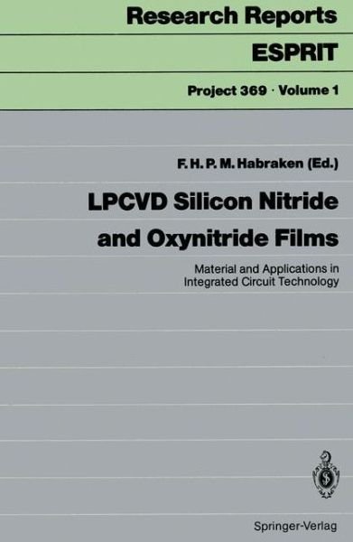
Lpcvd Silicon Nitride and Oxynitride Films: Material and Applications in Integrated Circuit Technology (Softcover Reprint of the Origi) F H P M Habraken Softcover Reprint of the Original 1st Ed. 1991 edition
Pedido desde almacén remoto
Nuestros clientes opinan:


Lpcvd Silicon Nitride and Oxynitride Films: Material and Applications in Integrated Circuit Technology (Softcover Reprint of the Origi)
F H P M Habraken
Description for Sales People: This volume, based on work done in an ESPRIT project, gives a broad overview of the chemical and physical characteristics of silicon oxynitrides, emphasizing how they influence the electrical behavior of this material, which is important for integrated circuit technology. Table of Contents: 1 Characterization of LPCVD Silicon Oxynitride Films.- Abstract.- I. Introduction.- II. Characterization Techniques.- III. Results and Discussion.- Bulk: Nitrogen, Oxygen and Chlorine.- Bulk: Hydrogen.- Interface: Oxygen and Nitrogen.- Interface: Hydrogen.- Structure.- IV. Concluding Remark.- References.- 2 Silicon Oxynitride Films: Ion Bombardment Effects, Depth Profiles, and Ionic Polarisation, Studied with the Aid of the Auger Parameter.- Abstract.- 1. Introduction.- 2. Experimental.- 3. Results.- Effects of Ion Bombardment.- Depth Profiling.- Line Widths and Shapes.- Auger Parameter Variation with O/(O+N).- 4. Discussion.- Ion Bombardment Effects and Ion Profiles.- Peak Widths.- Auger Parameter Variation.- 5. Conclusions.- References.- 3 Oxidation of Low Pressure Chemical Vapour Deposited Silicon Oxynitride Films.- Abstract.- I. Introduction.- II. Experimental.- Sample Preparation.- Oxygen Analysis.- Hydrogen Analysis.- III. Results.- Oxygen.- Hydrogen.- IV. Discussion.- Interface Reactions.- Oxidation Kinetics.- V. Conclusions.- References.- 4 Electrical Properties of LPCVD Silicon-Oxynitride Layers.- Abstract.- 1. Introduction.- 2. Sample Preparation.- 3. Charge Distribution in the Oxynitride Layer.- Measurement of the Charge Distribution.- One Step Deposited Layers.- Multi-step Deposited Layers.- 4. Interface Trap Density.- Interface Trap Density at Midgap.- Distribution of the Interface Trap Density.- Correlation between Dit and Qox.- Effect of the Oxynitride Deposition on the Interface Trap Density of an Underlying SiO2 Layer.- 5. Bulk Properties.- Relative Permittivity.- Charge Trapping.- Conduction.- Flatband Voltage-vs-Gate Voltage.- 6. Retention.- 7. Dielectric Integrity.- 8. Conclusions.- References.- 5 On the Correlation between the Electrical and Physico-Chemical Properties of LPCVD Silicon Oxynitride Films.- Abstract.- I. Introduction.- II. Summary of Experimental Results.- III. Discussion.- IV. The Model.- References.- 6 The Use of Oxynitride Layers in Non-volatile S-OxN-OS (Silicon-Oxynitride-Oxide-Silicon) Memory Devices.- Abstract.- 1. Introduction.- 2. Device Fabrication.- 3. Experimental Results and Discussion.- The Interface Trap Density.- Transient Behaviour.- Programming Voltages.- Retention Behaviour.- Endurance Behaviour.- Conclusions.- References.- 7 LPCVD Silicon Oxynitrides for LOCOS Isolation in CMOS Technology.- Abstract.- 1. Introduction.- 2. Experimental.- 3. Results and Discussion.- Patternability.- Ion Implant Blocking Efficiency.- Oxidation.- Birds Beak Formation.- Oxidation Induced Stacking Faults.- 4. Application to an Industrial Circuit Demonstrator.- Circuit Demonstrator.- Process.- Results.- 5. Conclusions.- References."Publisher Marketing: The present book collects a broad overview of chemical and physical char acteristics of silicon oxynitrides. Special emphasis is put on the way in which these properties influence the electrical characteristics and behaviour of this important material. The results presented here were obtained in an ex tended European research cooperation in the framework of ESPRIT Project 369 'Physical-chemical characterization of silicon oxynitrides in relation to their electrical properties', which ran from 1984 to 1988. In this project two industrial laboratories (Philips Research Laborato ries in Eindhoven, the Netherlands, and Matra Harris Semiconductors from Nantes, France) cooperated with various academic and government research laboratories (Harwell Laboratory in Great Britain, the Interuniversity Micro electronics Center (IMEC) in Leuven, Belgium, and the Faculty of Physics at the University of Utrecht in the Netherlands). The latter partner acted as prime contractor for the project. General interest in silicon oxynitrides for applications in integrated circuit technology stems from the fact that proper choice of deposition conditions enables one to produce materials with properties which can be either oxide like or nitride-like. Of, course, in I. C. technology one would like to combine the good properties ofthe two materials, i.e. superior electrical properties of silicon oxide and good diffusion barrier behaviour of silicon nitride, to men tion only a few, without paying for such an operation by obtaining all the less desirable properties in such a mixed material."
172 pages, 1 black & white illustrations, biography
![Cover for Carsten Rossi · Happiness Hacks: Das Anti-Digital-Detox-Buch: Wie digitale Medien Sie glucklich machen konnen (Paperback Book) [1. Aufl. 2025 edition] (2027)](https://imusic-static.b-cdn.net/images/missing-tall.png)
![Cover for Konrad Schmudgen · Unbounded Self-Adjoint Operators on Hilbert Space - Graduate Texts in Mathematics (Hardcover Book) [Second Edition 2026 edition] (2026)](https://imusic.b-cdn.net/images/item/original/822/9789402423822.jpg?konrad-schmudgen-2026-unbounded-self-adjoint-operators-on-hilbert-space-graduate-texts-in-mathematics-hardcover-book&class=scaled&v=1786374320)


![Cover for Handbuch Organisationssoziologie (Hardcover Book) [1. Aufl. 2021 edition] (2026)](https://imusic.b-cdn.net/images/item/original/191/9783658159191.jpg?2026-handbuch-organisationssoziologie-hardcover-book&class=scaled&v=1605099239)


